An App-note on Product Design using IFC6503 NanoSOM based on Snapdragon™ 660
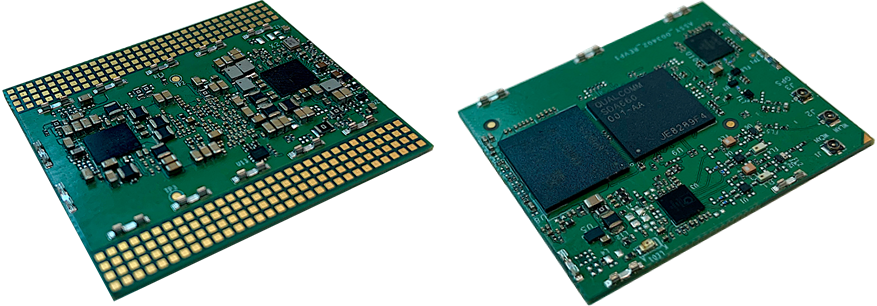
Penguin Edge recently added a new range of NanoSoMs in compact LGA packages to their product portfolio including the Inforce 6503, powered by the Snapdragon™ 660 Octacore processor. LGAs are land grid array packages with terminal pads on the bottom surface.
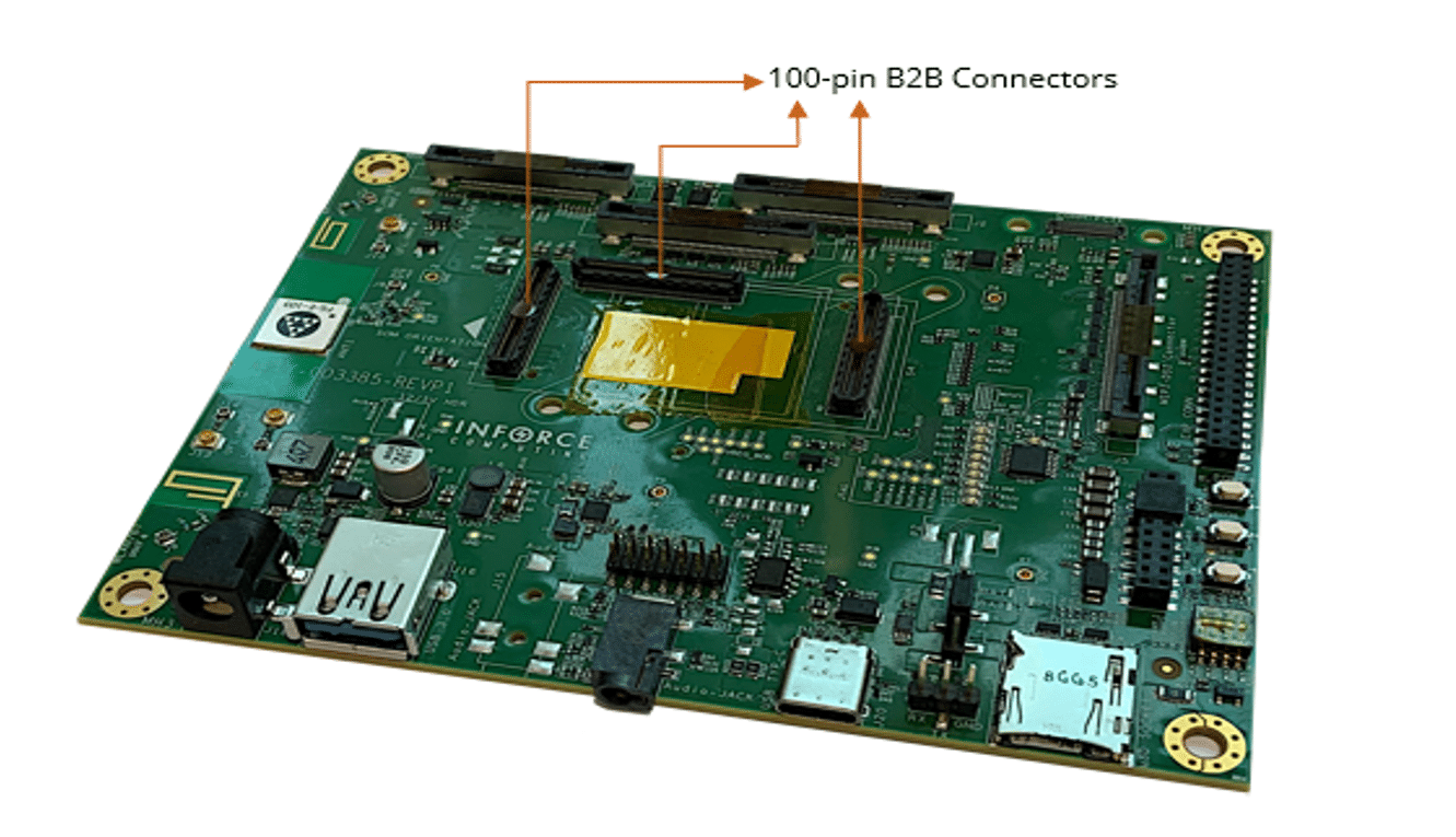
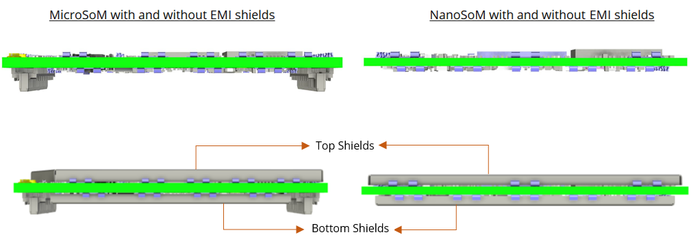
 These are leadless packages with electrical connections made via lands on the bottom side of the component to the surface of the connecting carrier board PCB. The LGA solder interconnect to the carrier is permanent and formed solely by solder paste applied at board assembly. It is thus different from our MicroSoM range of products that interconnects through a couple of board-to-board (B2B) connectors as illustrated below.
 This application note intends to provide our customers details and general guidelines on how to evaluate the Inforce 6503 NanoSoM using our reference designs to confirm functionality before they design-in the NanoSoM in to their product.
The LGA package has a few additional benefits no doubt, as compared to the B2B connectors and these are listed below:
 Smart wireless has created a reference carrier board for the Inforce 6503 NanoSoM, the ACC1C20, that specifically brings out all native interfaces of the Qualcomm® Snapdragon™ 660 including USB-C with full capability, to help create and optimize your products with the shortest turnaround time.
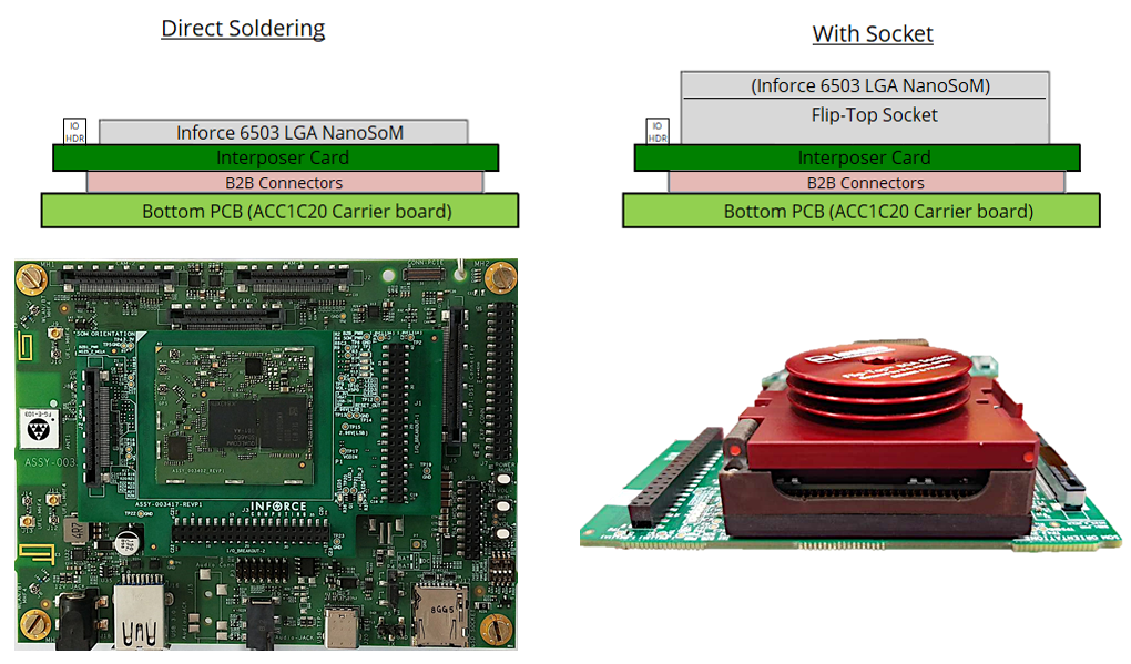
 The interposer card has the standard 100-pin B2B connectors on one side and forms the connection to the carrier board through these connectors. On the other side of this card, there is an option to either solder the LGA SoM directly or place it into a flip-top socket that is mounted on the card.
The reference design is therefore offered as two different SKUs, that either provide the NanoSoM soldered or socketed. With the socketed option of the reference design, you have the option to replace SoMs as necessary.
 The Inforce 6503 NanoSoM comes pre-loaded with a full featured Android Pie BSP software with support for the peripheral devices and I/Os listed below. All of these features can be validated with our reference designs on which the NanoSoM is either directly soldered or placed in the socket:
 These are leadless packages with electrical connections made via lands on the bottom side of the component to the surface of the connecting carrier board PCB. The LGA solder interconnect to the carrier is permanent and formed solely by solder paste applied at board assembly. It is thus different from our MicroSoM range of products that interconnects through a couple of board-to-board (B2B) connectors as illustrated below.
 This application note intends to provide our customers details and general guidelines on how to evaluate the Inforce 6503 NanoSoM using our reference designs to confirm functionality before they design-in the NanoSoM in to their product.
The LGA package has a few additional benefits no doubt, as compared to the B2B connectors and these are listed below:
- LGA SoMs have a lower mounted height owing to the absence of the B2B connectors. This allows more space above the device for a heat sink solution or for small form-factor applications.
- Board-level reliability can significantly exceed customer requirements.
- The durability of LGA SoMs in mechanical drop is typically greater than the MicroSoMs with B2B connectors.
- More features of the Snapdragon™ SoC can be brought out owing to the additional number of pins available
Inforce 6503 NanoSoM
 Smart wireless has created a reference carrier board for the Inforce 6503 NanoSoM, the ACC1C20, that specifically brings out all native interfaces of the Qualcomm® Snapdragon™ 660 including USB-C with full capability, to help create and optimize your products with the shortest turnaround time.
ACC1C20 Carrier
This carrier has the standard 100 Pin board-to-board receptacles as shown above. Considering that the Inforce 6503 SoM is a LGA package, it wouldn’t directly interface with the B2B receptacles. We have thus created an interposer card that forms the connection between the SoM and the carrier. The interposer card has the standard 100-pin B2B connectors on one side and forms the connection to the carrier board through these connectors. On the other side of this card, there is an option to either solder the LGA SoM directly or place it into a flip-top socket that is mounted on the card.
The reference design is therefore offered as two different SKUs, that either provide the NanoSoM soldered or socketed. With the socketed option of the reference design, you have the option to replace SoMs as necessary.
 The Inforce 6503 NanoSoM comes pre-loaded with a full featured Android Pie BSP software with support for the peripheral devices and I/Os listed below. All of these features can be validated with our reference designs on which the NanoSoM is either directly soldered or placed in the socket:
- Snapdragon™ 660 (SDA660) processor Octa-core Kryo™ CPUs running at 2.2GHz (Gold Cluster) and 1.8GHz (Silver Cluster)
- USB-C (USB 3.1/gen 1) with UltraHD display support; Input, OTG, MTP and mass storage devices
- USB-HS based input, MTP, camera and mass storage devices
- WiFi 802.11n/ac dual band (2.4 GHz and 5 GHz client functionality) and BLE 5.x with persistent MACs
- GPS
- Haptics Interface
- SD card access and eMMC memory, I2S and low speed peripherals(I2C/UART/SPI) through BLSP programming
- MIPI-DSI based displays with touch screen support
- Qualcomm SDKs’ support (SNPE, FastCV, Hexagon™, Adreno™)
- MIPI-CSI camera interface
- Analog and Digital audio
- Miracast
- RTC
- Control of user provisioned LEDs
- Android OTA update Procedure, Android Verified Boot(dm-verity) and Android Recovery
